Transport in Tube Reactors: Simplified Analysis
How do gases move around within a tube reactor? How is heat transported? To get some ideas, we'll perform a simplified transport analysis: rough estimates of the relevant velocities and characteristic times for the system. We'll consider a typical geometry and conditions for processing e.g. 150 mm diameter wafers*, e.g. for deposition of polysilicon.
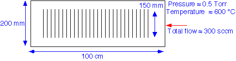
We assume as usual that the gases are ideal, with transport properties close to those of nitrogen. In this case, we take into account thermal expansion of the gases as they enter the reactor tube. To start with, let's examine transport of gases through the tube; we correct the tube cross-sectional area for for the wafer area, assuming negligible flow between the wafers.
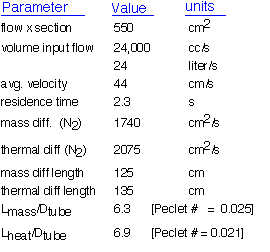
What do these results tell us?
The tube is radially isothermal. The thermal diffusion length is much larger than the radius of the tube: thus heat can easily travel by conduction from the walls of the tube to the central region. If the tube walls are held at a constant temperature, the radial temperature will be essentially constant. The axial temperature may vary and is somewhat influenced by convection (diffusion length comparable to the tube length), explaining the desirability of multi-zone heating.
Species concentrations are likely to be constant in the annular region: the mass diffusion length is much larger than the distance between the wafer edge and the tube. Convection will have little influence on species concentration. The concentration between the wafers will be considered separately.
Gas phase reactions have a few seconds to proceed: this allows one to choose which precursors can be used in such a system. Chemicals that will react in a few tens of milliseconds at the operating temperature will be consumed within a few cm of the hot zone; reactions that take more than 10 seconds won't contribute to deposition.
Simple Depletion?
Let's look at some plausible values for a polysilicon process running in the tube reactor above.
Parameter Value Units pressure 0.5 Torr temperature 600 C total flow 300 sccm wafer-wafer spacing 5 mm load length 75 cm wafers/load 150 exposed area [wafers+tube] 59300 square cm silane flow 120 sccm rate 75 A/min silane consumption 6.3x10⁻⁵ moles/second silane consumed 85 sccm
That is, 70% of the silane put into the reactor is consumed! This is a starved reactor. Depletion along the tube is very important. The diffusion length is comparable to the tube length, so axial diffusion has a modest but beneficial effect on axial uniformity.
Improvements in axial uniformity can be achieved by:
- Increasing the total silane flow: This requires increasing the total gas flows to maintain the same mole fraction. The cost of precursors goes up, and exhaust treatment becomes more demanding since less of the input silane is consumed in the reactor. Pumping speed may also limit the total flow that can be attained at a given pressure.
- Increasing the wafer spacing: The area of wafer to be deposited on per unit length of tube is decreased, but at the cost of reducing throughput, since fewer wafers are processed per batch.
- Changing the temperature along the tube: We can adjust heating zones to increase temperature as gases flow through the tube. The rate constant is lowered where the concentration is high and increased where the concentration is low. Such a scheme is fairly simple to implement, though it adds complexity to operation of the system.
- Dispense the precursor differently: We can dispense the silane in a distributed fashion along the tube, rather than simply sticking it in at one end. Such an approach requires an injector (typically of quartz) optimized to improve uniformity, usually in an empirical fashion. The injector is complex to fabricate, and will require periodic cleaning and eventual replacement, adding to the cost of operation of the system.
Between the Wafers
Convective flow between the wafers will be essentially negligible if the spacing is much less than the radius, which is normally the case. (As we've seen, convection plays little role in transport over small distances anyway.) Thus transport of reactants in the space between the wafers is essentially due to diffusion only.
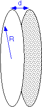
Since this is a CVD process whose purpose is to deposit a film on the wafers, it may also be assumed that the precursor is consumed on the wafer surfaces. Therefore transport between the wafers is described as simultaneous diffusion and consumption: Thiele diffusion. Recall that the solutions in the linear case are exponentials with a characteristic length:
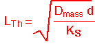
where Ks is the surface reaction rate constant. (In cylindrically symmetric geometries, the solutions will be modified Bessel function Io; these functions behave much like exponentials and don't change the qualitative conclusions.) If the Thiele length is much longer than the wafer radius, the concentration of the precursor will change little with radius and the film thickness will be fairly uniform along the radius of the wafer. In the other extreme film deposition will occur only on the outer ring of the wafer, for a distance roughly equal to Lth.
Let's consider a numerical example: for a typical polysilicon deposition process operating at the parameters shown above, a reasonable value of the reaction constant might be about Ks = 0.12 cm/second. Then for a 3 mm wafer spacing, Lth is about (1740*0.3/0.12)1/2 = 66 cm. The modified Bessel function Io is approximately (1+0.25x2) for small x=(r/Lth). Thus for a 150 mm wafer, r=7.5, x=7.5/66 = 0.11, and Io -1 = 0.003, i.e. about 0.3% variation in thickness to the wafer edge. A process running under these conditions is quite uniform. We can also see that if we increased the pressure to e.g. 5 Torr with the same molar flow and absolute silane concentration (i.e. reduced silane mole fraction), the Thiele length would decrease about 3-fold (due to the decrease in mass diffusion coefficient), and a much larger variation (about 3%) in thickness would result.
[reference: T. Badgwell et al J. Electrochem Soc 139 p. 524 (1992) ]
Since Lth controls the film uniformity, we can improve film uniformity by:
- Increasing wafer-wafer spacing: this is easy but reduces the throughput (number of wafers/batch.
- Increasing diffusivity: recall D goes as 1/P, so we can lower the pressure to improve uniformity: the "LP" in LPCVD.
- Decrease the reaction rate: changing precursors or changing the temperature may decrease the surface reaction rate constant, improving the film uniformity at the cost of decreased throughput (since the average deposition rate is lowered too). It might be possible to compensate by increasing the precursor concentration, if that does not induce undesirable gas phase (dust-generating) reactions.
Every trick is a tradeoff: the conditions that improve uniformity decrease throughput. This tradeoff is often encountered in industrial processes. There is almost by definition no simple solution, and empirical optimization is required. [Note that empirical uniformity improvements are particularly challenging since variation is by definition a positive number with a target of 0, so simple linear response-surface methods cannot be used. The author has found that extraction of the moments of variation from the wafer profile often produces linear responses in process conditions, making modeling much easier, but this approach is not in common use.]
We should note that more complex situations can arise in practice, in which deposition may depend on gas phase reactions taking place between the wafers, or be inhibited by reaction products. In such cases, the wafers are frequently enclosed in a "cage" of quartz with perforations, the size of which is empirically adjusted for optimal uniformity.
For a more detailed discussion consult "Fundamental Conceptions Modeling the Thickness Distribution of (LPCVD) Deposited Films on Wafers and within Narrow Trenches" , J. Schlote, K. Schröder, and K. Drescher , J. Electrochem. Soc. 138 p. 2393 (1991). Multivariate experimental methods are detailed in Statistics for Experimenters, Box, Hunter & Hunter, Wiley.
*OK, that’s how long ago I did this stuff. Multiply the size of the wafer by 2 (300 mm) and area by 4 to enter the modern world (2016).
Return to Tutorial Table of Contents
Book version of the CVD Tutorial