Gettering and Transport of Mobile Ions
Summary
Alkali metals such as Na and K in SiO2 often exist as small positive ions. In this state they move readily through thermal oxide under the influence of electric fields, even at room temperature: such motion within the gate oxides of MOSFETs will cause changes in threshold voltage and severely impact reliability.
Integrated circuit manufacturers use three approaches to solve this problem:
a) cleanliness in manufacturing: eliminating as many sources of Na and K as possible
b) gettering: Na and K will segregate into phosphorus-doped oxides
c) diffusion barriers: these contaminants diffuse much more slowly through silicon nitride, which can thus be used as an encapsulant to limit ambient contamination.
The combination of these three approaches has virtually eliminated practical reliability problems with sodium contamination, as evidenced by the virtual absence of literature on the subject since the early 1980's. However, recent data shows that modern IC's still contain significant amounts of process-induced sodium contamination within the BPSG layers: cleanliness alone is unlikely to be a sufficient guarantee of reliable IC operation. We were able to find no literature on other dopants for gettering positive mobile ions, or plausible alternative films. We can thus anticipate the use of internal gettering via phosphorus-doped oxides, combined with silicon nitride or PSG / nitride sandwiches for passivation, to continue for the foreseeable future.
Literature Review
General Remarks
Sodium is a common component of silicon dioxide: sodium oxides have been mixed with silicon dioxide to assist in the formation of glasses since ancient times, and "soda-lime" glass is commonly employed for structural glasses. Unfortunately for electronic applications, it is energetically favorable for oxygen to bond to silicon, leaving the Na atoms as ions within the matrix. These ions are partly neutralized by the slight negative charge on the O atoms in the lattice. They move very easily even through "dense" thermal SiO2 under the influence of an electric field. Thus, Na+ present in an oxide between a gate and a silicon surface (i.e. in a MOSFET) will move around when a voltage is applied to the gate, even at room temperature. The Na+ cannot penetrate the silicon lattice and thus can accumulate at the interface, leading to a net charge transfer and change in the threshold voltage of the device. This problem caused unacceptable instabilities in MOSFET operation until the role of Na+ ion drift was clarified in the mid-1960's [5,15]. (Other small positive ions such as potassium also play a role, but are less commonly found in the environment.) Figure 1 shows a schematic illustration of the problem. In normal operation (for e.g. NMOS) the gate attracts electrons to the surface of the silicon to turn the FET on. Initially, the positive ions are adjacent to the gate and thus have little effect on the device operation. However, after they drift to the silicon-silicon dioxide interface, they attract electrons and make the FET turn on prematurely: the threshold voltage of the device has changed. Unpredictable shifts in threshold voltage will wreak havoc upon digital logic, which depends on known and controlled voltage levels representing digital "1" and "0".
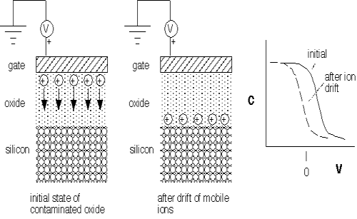
Figure 1: Effect of mobile ion motion under an applied field
Upon recognition of the origin of the problem, the first actions were removal of known sources of sodium contamination, including simple improvements in cleanliness related to human handling, to avoid the introduction of sodium from direct contact with contaminated solutions [6]. Furnace tubes were (and are) often made of bulk quartz, through which Na penetrates just as easily as when the oxide is grown on silicon; thus the regimen of Cl-based tube cleaning was introduced to prevent transport to the silicon during oxidation and diffusion. However, the most powerful means of limiting the mobile-ion problem was the use of phosphorus-doped oxides. Initially, these were formed by exposing thermal oxide to a phosphorus-containing environment prior to gate definition [4,7,8]. It was quickly established that the P-doped glass acted as a sink for Na and K ions, and that once captured into it they were only reluctantly released under the action of an electric field. Thus, MOSFETs "stabilized" by the introduction of phosphosilicate glass under the gate could be used in practical applications, as shown in figure 2.
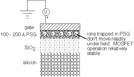
Figure 2: Early solution to mobile ion drift in MOS devices
2016 update:
Early authors assigned the gettering effect to the association of sodium ions with oxygen bound to phosphorus atoms [3,4,8]. Elemental phosphorus oxidizes in trivalent or pentavalent forms (P2O3 and P2O5), the latter being that commonly encountered when excess oxygen is present. Oxidized phosphorus was believed to incorporate substitutionally into the silicon dioxide lattice (at least at low concentrations), which consists of tetrahedra of SiO4, with each oxygen bridging to a neighboring silicon. Thus some phosphorus atoms would have an oxygen with net negative charge, associated with a sodium ion. The model is depicted schematically in figure 3(a). However, more recent work based on Raman spectroscopy and other techniques has shown that most of the phosphorus is present in the same state as its own oxide (with three bridge bonds and one double-bonded oxygen). It is known that at high concentrations of phosphorus, sodium stabilizes the formation of six-coordinated silicon atoms [18,19], as shown in figure 3(b), but it’s not clear if this is relevant at the very low phosphorus concentrations used in electronic applications. So it’s a bit unclear what the actual gettering mechanism is at this point!
We note in passing that although we have not yet found literature on the subject, it is quite reasonable that arsenic-doped oxides will getter ionic contaminants, since the chemistry of As and P is quite similar. However, B is incorporated into the silicon dioxide lattice in a trivalent form, and is electron-deficient (thus in effect positively charged); indeed, many boron compounds are strongly electrophilic. There is no cause to expect that boron glasses will show particular affinity for positive ions, and no indication in the literature that they do.
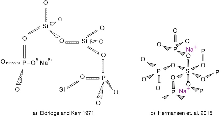
Fig. 3: Position of trapped sodium ion in mixed silica/phosphorus oxide glass matrix: a) early ideas; b) more recent structural analysis.
The placement of the PSG between the gate and thermal SiO2, while easily implemented, had several serious limitations. The thickness of the PSG layers was typically 100-200 Å. Higher sodium concentrations are more easily released due to the fact that the trapping sites vary in energy. The deepest sites are filled first, with less favorable sites occupied as ions are added; these later additions escape readily under the influence of an electric field [4,8]. Thus, it was desirable to create high phosphorus concentrations to ensure trapping, but at high P concentrations the glass itself acquires a bulk polarization under sustained electric fields, again leading to threshold shifts [3]. Further, since the PSG is between the gate and the silicon surface, charge trapped within it still influences the threshold voltage of the device, causing a reduced but not negligible sensitivity to contamination.
These problems were solved by depositing the PSG through chemical vapor deposition after the formation of the MOSFET [1]. The removal of the gettering layer from the MOSFET eliminates the effects of any trapped ions on FET operation, and allows much thicker layers with lower phosphorus concentration, improving the total tolerance for contamination without introducing susceptibility to polarization. Deposited PSG also softens at a much lower temperature than undoped glasses; the use of flow for planarization led to the almost universal use of PSG and later BPSG as the first deposited dielectric layer in early CMOS processes, conferring the joint benefits of planarization and mobile ion protection.
Unlike silicon dioxide, silicon nitride has a dense structure without the internal micropores that allow easy transport of ions. [16] Thus, silicon nitride can be used to prevent in-diffusion of sodium from the environment. Early CMOS IC's thus employed both one or more BPSG layers deposited prior to first metallization, and a passivation layer containing various combinations of PSG and silicon nitride. This configuration, combined with modern clean process procedures and materials, has resulted in a robust integrated-circuit technology, with the predominant problems in MOSFET operation related to trap formation in the thermal oxide rather than mobile ion drift, as evidenced by the rarity of literature on mobile ion issues in the 1980's and 1990's.
The evolution of processing to lower temperatures has tended to eliminate the use of BPSG for processes after about 250 nm gate length, but the use of passivation layers composed of nitride and doped oxides is still popular (2016). Modern IC’s use a seal ring structure, where a continuous metal barrier at the perimeter of the IC blocks penetration of contaminants into the exposed passivation edges, and the passivation layer blocks penetration through the metal sandwich from the top surface.
However, the need for gettering of mobile ions has not been removed. Measurable ionic contaminants can be introduced in front-end processing [2], and that parts obtained from a wide variety of vendors contain peak sodium concentrations of 1017 to 1019 atoms/cm3, as measured by SIMS, apparently often introduced through relatively dirty back-end processing [9,14]. Floating-gate memory devices are an exquisitely sensitive test of mobile ion control, since they rely on a floating gate with a "permanent" electric field (and thus a permanent attraction for mobile ions). Internal sources of moisture (e.g. PETEOS films) can cause the release of trapped mobile ions in BPSG layers through reactions of the general form P=O => P-OH, destabilizing any associated sodium ions.
The released sodium ions then can migrate to negatively charged floating gates, neutralizing them and impacting charge retention performance of the memory. [12] While this particular problem is solved in practice by interposing a moisture barrier layer between the devices and the intermetal dielectric layers, the observed degradation demonstrates that commercial products can contain significant amounts of mobile ion contamination, and require effective gettering to achieve reliable operation.
Furthermore, the presence of underlying gettering layers does not completely protect an IC from ambient contamination: apparently, Na can diffuse readily along metal lines to the field oxide level and then proceed laterally to FET gate regions [10]. Thus passivation layers remain indispensable to protect the devices from relatively uncontrolled ambients. It appears that defect-free PSG is an excellent passivating layer [10], but that cracking related to tensile stress in the film, or poor sidewall integrity, leads to ready penetration of both oxide and nitride passivation films by ambient contamination. [10, 13].
We can conclude that the combination of clean process techniques, internal mobile ion gettering, and passivation protection layers, which has successfully served the industry for the last two decades, will continue to be employed in the foreseeable future. The replacement of BPSG flow with chemomechanical polishing for planarization will moderate requirements on phosphorus doping levels but will not lead to the abandonment of doped glass layers for mobile ion protection.
Metrology
O2+ SIMS:
Secondary Ion Mass Spectroscopy has good sensitivity for Na and K; useful for monitoring total contamination in e.g. oxide layers. This method measured the atoms present rather than their electrical state, and does not therefore distinguish between mobile ions and trapped neutral species. Ions will move under the influence of the electric fields created by the incoming positive ion beam during sputtering; in order to obtain believable information on the spatial distribution of contaminants, it is necessary to flood the sample with electrons during analysis to avoid net charging.
Other (less convenient) analytical methods are use of radioactive Na22, neutron activation analysis, and flame photometry.
TVS:
Triangular Voltage Sweep is an electrical technique, and thus requires at least a completed MOS structure. The displacement current due to the movement of the ions is measured while applying a voltage which increases linearly with time, with the device held at an elevated temperature (typically 200-300°C). This method is of course only sensitive to mobile species and does not necessarily reveal the identity of the moving charge. It is fast and sensitive (with a minimum detectability of about 10-9 charges/cm2). [17]
The most common alternative electrical characterization method is bias-temperature stress, in which the C-V curve of an MOS capacitor is measured at room temperature, and then the device is placed under bias and raised to an elevated temperature. After allowing ions to drift, the device is cooled under bias and the C-V curve remeasured; the shift in the flatband voltage (refer to figure 1 above) measures the amount of charge present. This technique is accurate but cumbersome to perform.
Automated capacitance-voltage systems for implementing both these measurements are commercially available from multiple vendors.
=============================
May 2016: Thanks to Olivier Castany for pointing out the problems with the pentacoordinated phosphorus structure shown in the original version of this short.
References
- "Advantages of Vapor-Plated Phosphosilicate Films in Large-Scale Integrated Circuit Arrays", M. Schlacter, E. Schlegel, R. Keen, R. Lathlaen and G. Schnable [Ford Microelectronics], IEEE Trans El Dev ED17 1077 (1970)
- "Removal of Alkaline Impurities in a Polysilicon Gate Structure by Phosphorus Diffusion", C. Pearce, J. Moore and F. Stevie [AT&T Bell Labs], J. Electrochem. Soc. 140 1409 (1993)
- "Polarization Phenomena and Other Properties of Phosphosilicate Glass Films on Silicon", E. Snow and B. Deal [Fairchild], J. Electrochem. Soc. 113 263 (1966)
- "Sodium Ion Drift through Phosphosilicate Glass - SiO2 Films", J. Eldridge and D. Kerr [IBM], J. Electrochem. Soc. 118 986 (1971)
- "Ionic Contamination and Transport of Mobile Ions in MOS Structures", M. Kuhn and D. Silversmith [Bell Labs], J. Electrochem. Soc. 118 966 (1971)
- "Transfer of Mobile Ions from Aqueous Solutions to the Silicon Dioxide Surface", S. Raider, L. Gregor and R. Flitsch [IBM], J. Electrochem. Soc. 120 425 (1973)
- "Complete Removal of Sodium from Silicon Dioxide Films by Formation of Phosphosilicate Glass", D. McCaughan, R. Kushner and S. Wagner [Bell Labs], J. Electrochem. Soc. 121 724 (1974)
- "Phosphosilicate Glass Stabilization of FET Devices", P. Balk and J. Eldridge [IBM], Proc IEEE 57 #9 p. 1558 (1969)
- "Built-in reliability Through Sodium Elimination", J. Chinn, Y.-S. Ho and M. Chiang [Siliconix], IEEE Intl Reliability Phys Symp 1994 p. 249
- "The Impact of an External Sodium Diffusion Source on the Reliability of MOS Circuitry", P. Hefley and J. McPherson [TI], IEEE Intl Reliability Physics Symp 1988 p. 167
- "The impact of intermetal dielectric layer and high temperature bake test on the reliability of nonvolatile memory devices", E. Sakagami, N. Arai, H. Tsunoda, H. Egawa, Y. Yamaguchi, E. Kamiya, M. Takebuchi, K. Yamade, K. Yoshikawa and S. Mori [Toshiba], IEEE Int'l Reliability Physics Symposium 1994 p. 359
- "Phosphorus Migration Kinetics from PSG to Glass Passivation Surface", G. DiGiacomo [IBM], 1984 IEEE Int'l Reliability Physics Symposium p. 223
- "Comparison of passivation films: The effect of thermal cycles and comparison of phosphorous doped oxide films", T. Wu , K. O'Brien and D. Hemmes [Motorola, Novellus], J Vac Sci Technol B11 #6 2090 (1993)
- "Mobile Ion Reduction in Interlevel Dielectrics Through the Optimization of Unit Processes", W. M. Lee, J. Chinn [EKC], VMIC 1995 poster paper
- "Ion Transport Phenomena in Insulating Films", E. Snow, A. Grove, B. Deal and C. Sah [Fairchild], J. Appl. Phys. 36 1664 (1965)
- "Sodium diffusion in plasma-deposted amorphous oxygen-doped silicon nitride (a-SiON:H) films", J. Osenbach and S. Voris [Bell Labs], J. Appl. Phys. 63 4494 (1988)
- Semiconductor Material and Device Characterization, D. Schroder, Wiley 1990 (ISBn 0-471-51104-8), p. 262 ff.
- “Structure-topology-property correlations of sodium phosphosilicate glasses”, C. Hermansen, X. Guo, R. Youngman, J. Mauro, M. Smedskjaer and Y. Yue, J. Chem Phys. 143 064510 (2015)
- “Structure and formation mechanism of six-fold coordinated silicon in phosphosilicate glasses”, D. Miyabe, M. Takahashi, Y. Tokuda, T. Yoko and T. Uchino, Phys Rev B71 712202 (2005)
Selected Shorts Table of Contents