Fixed Charge in Deposited Oxides
Summary
Various reports in the literature have described problems encountered in the use of SOGs, PETEOS layers, and PETEOS BPSG, related to the creation of large positive charges affecting isolation below the underlying field oxide.
Three factors seem to be of importance for creating high fixed charges:
- high carbon incorporation
- presence of a source of hydrogen (plasma nitride or CVD nitride)
- high temperature anneal
In one case direct SIMS measurements showed that the result was transport of carbon to the Si/thermal SiO2 interface, corresponding to the electrical location of the charge. Other work indicates that bulk positive charge can exist in deposited oxide or SOG.
Plasma deposition may contribute to charging problems, but surface damage from ion bombardment does not seem to be the mechanism.
The following guidelines should be followed to avoid large fixed charge in oxides, especially when post-deposition temperatures exceeding 600°C are expected:
- minimize carbon (probably -CxHy) content in the deposited film
- minimize hydrogen in all forms (Si-OH, H2O[ads], Si-H)
- maximize deposition temperature (>300°C)
- exploit Si-rich stoichiometry
Process integration concerns are:
- overlying or underlying sources of carbon or hydrogen
- subsequent anneal temperature and ambient
Literature Review
Introductory Remarks
Charges in oxides may influence the condition of an underlying silicon surface if they are not screened by intervening conductors. For example, the (old) LOCOS isolation process depends on the field oxide having a sufficiently large threshold voltage to avoid the formation of a conducting channel beneath it. For example, significant positive charge in an overlying dielectric layer may attract electrons to the surface and impact isolation between neighboring devices, as shown schematically in figure 1.
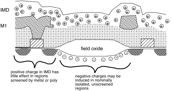
Fig. 1: Charge in IMD influences surface potential and charge density under unscreened field oxide
Thermally grown oxides typically have from mid-1010 to 1-2x10¹¹ positive charges per cm2, localized within about 35 Å of the Si/SiO2 interface [10]. Total charge densities much smaller than this will therefore have no significant effect on device performance.
Carbon And...
Various deposited oxides are widely employed for interlayer and intermetal dielectrics over field oxide, as spacers in low-doped-drain (LDD) MOSFETs, and for filling of isolation trenches.
Several recent publications have discussed the occurrence of large threshold shifts in field devices or other process problems related to excessive positive charge (>1012/cm2) in deposited oxides. In every case, mere deposition of a film or application of a spin-on glass (SOG) was insufficient to cause a problem; a confluence of at least two factors was required. Table I summarizes the situation: in each report, all the factors shown in a given row were necessary to give rise to an objectionable charge related to the deposited oxides.
Table 1: Factors in formation of large fixed charge
reference
oxide layer
carbon
hydrogen
anneal temp
Hsu 1993 [1]
silicate SOG
PETEOS
silicate SOG?
<450°C?
Pramanik 1989 [2]
PE SiH4 [?]
siloxane SOG
PE nitride
Å450°C
Wilson 1992 [3]
[goes with Carlson]
Carlson 1993 [4]
PETEOS
PETEOS
--
900°C (O2/HCl)
1000°C (N2)
Kuo 1992 [5]
silicate SOG
PETEOS
PE nitride
<450°C?
van Schr. 1995 [6]
PETEOS
PETEOS
--
900°C (O2)
Mori 1994 [7]
BPTEOS
BPTEOS
CVD nitride
850°C [N2?]
Nguyen 1990 [12]
PETEOS
PETEOS
> 600°C
PETEOS
PETEOS
high RF power
TEOS/O3
TEOS/O3
> 600°C
Ibok 1991 [18]
BPTEOS
BPTEOS
900°C
Liu 1991 [19]
silicate SOG
PETEOS
PE nitride
410°C
In figure 2 we schematically summarize the conditions under which large threshold shifts are observed for low anneal temperatures; in figure 3 we depict the situations leading to threshold shift for high anneal temperatures.
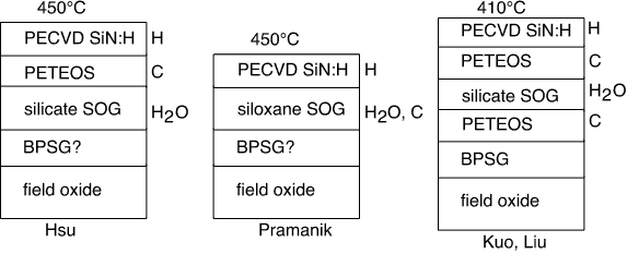
Figure 2: Bad Actors Gallery, Anneal < 500°C
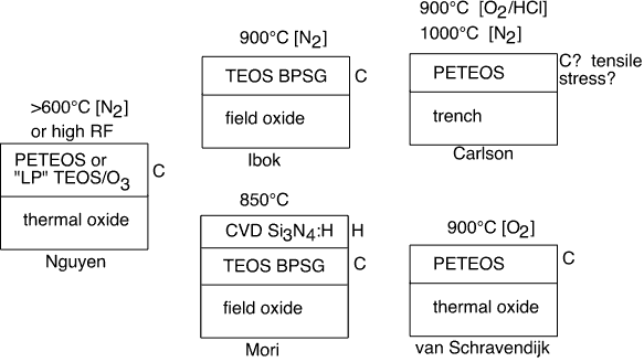
Figure 3: Bad Actors Gallery, Anneal > 500°C
It appears that the conjunction of water, carbon, and hydrogen are required for problems to occur for temperatures < 450°C, and only carbon (and perhaps water) are needed for T>600°C. Are there alternative explanations? Carlson et. al. associated flatband shifts in a trench isolation structure with compressive stresses in the as-deposited PETEOS oxides (probably from Novellus and AMT reactors), but Van Schravendijk et. al. varied the [C] in PETEOS films by varying O2:TEOS ratios, with LF power adjusted to maintain constant stress. They found that threshold shifts after a 900°C anneal in PETEOS films were just linearly related to the [C] in the film by SIMS. Based on van Schravendijk et. al., we suggest that the changes made to render the films tensile (reduced RF power, probably also lower deposition rate, possibly increase in O2 in the mixture) will also reduce the carbon concentration in the films. We note that Carlson et. al. used an O2:TEOS ratio of 2.22 in the putative Novellus reactor, which van Schravendijk et. al. find to give very large carbon incorporation. Further, their figure 7 shows that the flatband voltage shift changes drastically for the better at higher O2:TEOS ratios, exactly consistent with the findings of van Schravendijk.
What role does radiation damage play? The work of Pramanik et. al. involved siloxane SOG, which typically contains Si-CH3 or larger radicals, but rarely unsaturated bonds. In Kuo et. al. a PETEOS oxide was present in combination with a silicate SOG: the conditions of deposition are not given but we can guess that the PETEOS contains significant carbon contamination, whereas the SOG is probably a source of H2O. In both cases a plasma oxide is deposited directly on the SOG, creating some possibility of bond breaking at the interface, as proposed by Kuo et. al. However, Pramanik notes that thicker SOG created a larger problem, inconsistent with a large role for interfacial effects. The observation of large threshold shifts in non-plasma films by Nguyen and Murarka also argues against bombardment effects playing a role.
Nguyen and Murarka [12] report large threshold shifts resulting from deposition of both PETEOS and thermal TEOS films on top of thermal oxide after anneals at elevated temperature (600-1000°C). The plasma TEOS films also show large threshold shifts as deposited when high power densities are employed. The thermal TEOS films are fairly well-behaved as deposited but again show large shifts when annealed. The deposition conditions for the thermal films (60 Torr total pressure) are likely to lead to significant carbon incorporation in the films. Although it is unclear what amount of TEOS (as opposed to carrier gas) is being delivered to the chamber, the high deposition rates argue for relatively low O2:TEOS ratios in the plasma films, again suggesting significant carbon incorporation according to the work of Carlson et. al. [6].
We find therefore that in each case in which a large threshold shift is reported in a field device due to a deposited film, carbon is present, and either interacts with a source of hydrogen or is annealed at a temperature>600°C (although [12] perhaps higher RF power in plasma depositions can substitute for the anneal).
It is worth noting that the amount of fixed charge is a very small fraction of the amount of C. For example, using the work of Mori et. al., a typical carbon concentration of 1020/cm3 in a TEOS oxide 2000 Å (2x10⁻⁵ cm) thick corresponds to an areal concentration of 2x10¹⁵/cm2. The measured threshold shift of 20 V for an 8000 Å thick layer corresponds to a charge density at the interface of about 6x10¹¹/cm2. Thus less than 1 in 3000 carbon atoms participate in charge formation.
Where is the charge located? Mori et. al. found specifically that the location of the positive charge was at the silicon / thermal oxide interface, whereas in a very similar experiment Ibok et. al. found evidence for bulk rather than surface charge. Pramanik et. al. report that their leakage problems were suppressed by etching the passivation nitride away, suggesting that in this case the leakage was not located within the field oxide, and may be reversibly associated with the presence of H.
Counterexamples
The selection of reports described above support the generalization that fixed charge problems are absent or unobjectionable in the absence of a source of carbon and some other catalyzing event. Possible exceptions are discussed below.
Liu et. al. [18] cite PETEOS as the problem in most of their work. However, they briefly note that PECVD oxide (from SiH4?) can be a problem if the refractive index is "low", and that "Si-rich" layer from either TEOS or SiH4 (apparently as evidenced by a "high" refractive index) is well-behaved. It seems unlikely that a truly silicon-rich TEOS oxide can be easily created, since the silicon is fully oxidized and will not be readily reduced. Patrick et. al. [20] show that the refractive index of PETEOS films deposited at high temperatures increases quite noticeably for high O2:TEOS ratios (their figure 2). While no details are given in Liu's report on TEOS deposition conditions, it seems quite likely that their initial work was done at low O2 flows by reference to the approximately contemporaneous work of Carlson et. al.; if so, increasing oxygen flows would have given a higher refractive index (and a lower deposition rate!), but at the same time would very likely reduce carbon incorporation, and is thus quite consistent with our thesis.
It is harder to explain away the remark that "low index" (SiH4) oxides were also a problem. Here there is no obvious source of carbon contamination. Unfortunately, absolutely no details are provided in the reference, nor is this exception mentioned in the later work of Kuo et. al. [5] which appears to involve some of the same authors.
Nishi et. al. [11] deposited PETEOS oxides on silicon at fairly low rates and high oxygen:TEOS ratios (Å18:1), obtaining charge densities of about 3-8x10¹¹/cm2 for a 1000 Å oxide. In this case, although it seems very reasonable that the deposited film was relatively free of carbon, the substrates were HF-cleaned silicon and probably contained a native oxide grown during deposition setup, annealed at 440°C. We cannot disentangle the fixed charge due to this low-quality interface from that added by the deposited oxide, since the authors used only one deposited oxide thickness. If all the charge is bulk charge in the deposited oxide, the measured values could represent a serious problem for thick (0.5 - 1 µm) intermetal dielectrics, but it is quite plausible that most or all is associated with the interface and doesn't scale with oxide thickness.
Li et. al. [8] report a large flatband shift towards negative voltage for LPCVD PSG from SiH4. The shift occurs between about 150 and 700°C, and is somewhat correlated with the release of hydrogenous species (just what they are is not clear, since nuclear reaction profiling was used and gives only total H, not the chemical state). This report does not give absolute charge densities or provide measurements on e.g. annealed thermal oxides from which we might infer them. Thus we can't be sure whether the changes in threshold are the formation of positive charge in the oxide, or the neutralization of negative charge. If in fact the charge state relaxes to 0 after a 750°C anneal, such a phenomenon could exist quite frequently in commercial PSG and BPSG films without causing a practical problem: films near the semiconductor are always densified at 700-800°C and usually flowed at 850-950°C, and passivation films are probably effectively screened from the underlying MOSFETs by the multiple metal layers. Nevertheless, this report suggests that the presence of hydrogen may play a role in charge formation and transport.
Discussion
Formation of a net charge within an oxide requires both that charged states exist and that charge transport can occur to a conductive surface. When defects are created by e.g. radiation damage, it is easy to imagine that an electron may gain sufficient energy (typically several eV) to enter the oxide "conduction band" and thus stand a fair change of being transported through the oxide to a gate or substrate. However, annealing at moderate temperatures, and the action of chemical agents, seem less likely to accomplish such a feat: we should consider possible molecular means of charge transport.
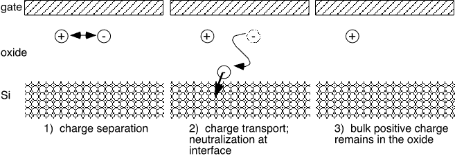
Figure 4: Generation of bulk charge in an insulating oxide
Positively-charged states in silicon dioxide related to an unpaired electron have been studied extensively by ESR (electron spin resonance) [14]. A variety of defect sites exist, but all are related to oxygen vacancies or Si-Si bonds: that is, they are associated with a "Si-rich" region in the film. While most ESR work appears to deal with radiation damage in oxides, one may also plausibly associate Si dangling bond formation with the interaction of an Si-H bond and OH radicals created from water associated with e.g. P2O5, thus:
Si-H + OH => Si- + H2O
with the subsequent formation of OH-, acting to charge the site and transport the resulting electron to an interface.
Films created by thermal CVD from SiH4 at low pressures are likely to have significant Si-H bonds. Undoped films will contain little Si-OH and not be particularly hygroscopic, but 7 wt.% PSG might result in significant accumulation of water within the film once exposed to atmospheric moisture. The combination of these two circumstances might explain formation of positive charges in LPCVD PSG as observed by Li et. al.; one would then not expect to encounter large charge densities in e.g. APCVD films, where little or no Si-H is found (i.e. the films are generally highly oxidized).
What role might be played by carbon? Elschenbroich [9] points out that the Si-C bond is not strongly polar and rather immune to attack by most reagents. The non-polarity of the bond suggests that it would not result in charge separation when broken. The O-C bond in an Si-O-C linkage is more polar and more easily attacked, although it is a fairly strong bond (86 Kcal/mole [13 p. 1195]). The polarity of this linkage makes charge separation more plausible when the bond breaks. If we assume that the active agent at low temperatures is monatomic H evolving from the plasma nitride, we are led to consider simple substitution reactions of the form:
Si-O-CH3 + H2 => Si-OH + CH4
The movement of neutral methane to the Si interface, followed by charging from the Si, would explain the results of Mori et. al. [7]. However, the formation of mobile positively-charged carbocations would lead to a net negative charge in the oxide if they were able to move to an interface and be neutralized. In order to explain a positive oxide charge we must invoke a mobile negative moiety. This is unlikely to be hydrogen. More plausible candidates are OH- and O-; we might envision a reaction like:
Si-O-CH3 + H2 => Si-OH- + CH3+
followed by
Si-OH- + OH => Si-OH + OH-
with the charged hydroxyl radical able to transport an electron through the oxide to a conductive surface. The alkyl is then left behind as a bulk positive charge. Any mechanism involving a charged alkyl should occur much more readily for larger alkanes (ethyl or propyl vs. methyl) and even more so for secondary and tertiary alkanes (e.g. [13 p. 176 ff]).
High-temperature anneals in the absence of excess hydrogen can lead to formation of unsaturated species from ethyl and larger alkyls, i.e.
Si-O-CH2H3 => Si(-OH)(C=CH2) + H2
Unsaturated alkenes are much more reactive than their saturated alkane brethren, due to the exposed pi electrons of the double bond: they can be more readily attacked by electrophilic species such as oxygen. Plasmas may also generate unsaturated species, as well as various radicals, in the gas phase during deposition.
Transport of negatively charged organic species seems less likely: stabilization of charged states in organics typically requires larger molecules, with correspondingly low mobility. Small organic acids (e.g. formic, HCOOH) could release H+ and become negatively charged (HCOO-), but it seems likely that the monatomic hydrogen would be much more mobile than the large cation, leading to a net negative charge in the oxide.
It is not apparent that plasma damage, due to ion bombardment of surfaces, plays a significant role. Joubert et. al. [15] showed that UV from a high-density ECR oxygen plasma led to the creation of a large fixed positive charge in thermal oxide. Similar results were obtained for ECR deposited oxides at quite low temperatures, but deposition at 300°C, or a modest anneal (350°C) was adequate to eliminate most of this charge, despite the very large bombardment effects occurring at the oxide surfaces during deposition. The Lam Epic process operates at a nominal temperature of about 265°C and has been successfully employed in IMD applications with no reports of field threshold problems. Conventional low-density plasmas create 100 to 1000 times less radiation than typical high density sources, so UV-related damage is unlikely to occur very much and would be easily annealed. Ion bombardment, despite the fact that it must result in significant atomic displacement in the near-surface region of the film and that it may lead to finite voltages across the oxide and resulting bulk charge transport, does not appear to intrinsically result in large fixed oxide charges. We are led to suggest that such charging problems as are observed with plasma oxides are more likely to be chemical than physical in origin. The presence of a plasma will increase the likelihood of incorporation of carbonaceous species through the formation of radicals in the plasma, and can form unsaturated species (C=C double bonds) where none were present initially. In SiH4-based processes plasmas may encourage the creation of higher silanes (e.g. Si2H6), which if unoxidized cause the incorporation of Si-Si bonds into the oxide, perhaps acting as potential positive charge centers.
In summary, we suggest the following guidelines for avoiding large fixed charge in oxides:
- minimize carbon (probably -CxHy) content
- minimize hydrogen in all forms (Si-OH, H2O[ads], Si-H)
- maximize deposition temperature (>300°C)
- avoid Si-rich stoichiometry
Process integration concerns are:
- overlying sources of hydrogen may interact with any carbon in an IMD film
- subsequent annealing temperatures and environment are important: temperatures higher than 600°C, and oxygen-containing ambients, will exacerbate any potential charge problem.
Metrology
Fixed Charge: most easily measured by observing the flatband shift in the high-frequency C-V curve of an MOS capacitor, as shown in figure 2 below. The position of the "theoretical" curve depends on the nature of the top electrode (poly, aluminum, Hg dot, etc.) The deposited oxide should lie atop a thin, annealed thermal oxide on lightly-doped silicon, to ensure a reasonably good interface. The location of the charge can be established by varying the thickness of the deposited oxide or etching it with repeated measurements: charge localized at the Si/SiO2 interface will give a threshold shift linear in the total oxide thickness, whereas bulk oxide charge will give a quadratic behavior. Mobile charges can also contribute to the threshold shift, and must be separately characterized by e.g. bias-temperature stress or TVS measurements. See [15].
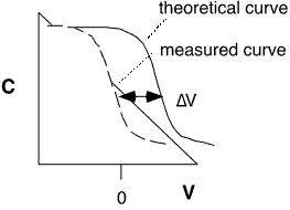
Figure 5: Capacitance-voltage curves
Carbon: Total carbon is conveniently measured by SIMS. FTIR will detect many carbon-containing bonds but sensitivity is rather poor.
Hydrogen: FTIR is effective for large concentrations of Si-H, Si-OH, and H2O. Moisture evolution analysis gives total water content with better sensitivity and quantitation than FTIR. Thermal desorption analysis can also detect hydrogen.
References
- "Field Inversion Generated in the CMOS Double-Metal Process Due to PETEOS and SOG Interactions", S.-L. Hsu, L.-M. Liu, C.-S. Fang, S.-L. Ying, T.-L. Chen, M.-S. Lin, and C.-Y. Chang, IEEE Trans. El. Dev. 40 49 (1993)
- "Field Inversion in CMOS Double Metal Circuits Due to Carbon Based SOGs", D. Pramanik, S. Nariani, G. Spadini [VLSI], 1989 VMIC Conference, Santa Clara, p. 454
- "Characterization of TEOS oxides used in the isolation module of high-speed bipolar and BiCMOS circuits" S. Wilson and H.-B. Liang [Motorola], Thin Solid Films 220 59 (1992)
- "Deposition Method to Control Plasma-Enhanced Chemical Vapor Deposition Tetraethylorthosilicate Oxide Charge" A. Carlson, T. Wu, and H.-B. Liang [Motorola], J. Electrochem. Soc. 140 774 (1993)
- "Intermetal Dielectric-Induced N-Field device Failure in Double-Level Metal CMOS Process", H. Kuo, K. Lin, C. Liu, R. Tsai, M. Lin and C. Yoo (TSMC), IEEE ED Letters 13 405 (1992)
- "The Role of Carbon in PECVD TEOS Films", B. van Schravendijk, D. Carl, F. Nagy and W. van den Hoek [Novellus], NCC AVS TFUG/PEUG Joint Meeting 4/13/95
- "Analysis of Isolation Degradation Induced by Interlayer Material in Capacitor Over bit-Line (COB) DRAM Cell", H. Mori, K. Shibahara, K. Koyama and N. Kodama [NEC], Ext. Abstr. 1994 Intl Conf Solid State Devices and Materials (Yokohama) p. 904
- "Annealing of Low Pressure Chemical Vapor Deposited Phosphorus Glass Films -- Effect on Electrical Properties and Concentrations of Hydrogen Containing Species", S. Li, S. Murarka, X. Guo, W. Lanford, J. Electrochem. Soc. 139 2599 (1992)
- Organometallics: A concise introduction (2nd. ed.), C. Elschenbroich , VCH 1992 [ISBN 0-89573-983-6]
- Silicon Processing for the VLSI Era (Vol I), S. Wolf and R. Tauber, Lattice Press 1986 [ISBN 0-961672-3-7], p. 223
- "Characteristics of Plasma-Enhanced Chemical Vapor Deposition Tetraethylorthosilicate Oxide and Thin Film Transistor Application", Y. Nishi, T. Funai, H. Izawa, T. Fujimoto, H. Morimoto and M. Ishii [Sharp], Japn. J. Appl. Phys. 31 part 1, 4570 (1992)
- "Properties of (CVD) tetraethylorthosilicate oxides: Correlation with deposition parameters, annealing, and hydrogen concentration", A. Nguyen and S. Murarka (RPI / Applied Materials ), J Vac Sci Technol B8 533 (1990)
- Introduction to Organic Chemistry, 2nd edition, A. Streitweiser and C. Heathcock, Macmillan 1981 [ISBN 0-02-418050-5]
- "Paramagnetic Point Defects in Amorphous Thin Films of SiO2 and Si3N4: Updates and Additions", E. Poindexter and W. Warren, J. Electrochem. Soc. 142 2508 (1995)
- "Influence of ion energy on the physical properties of plasma deposited SiO2 films", O. Joubert, R. Burke, L. Vallier, C. Martinet, and R. Devine [CNET], Appl. Phys. Lett. 62 228 (1993)
- [deleted]
- Semiconductor Material and Device Characterization, D. Schroder, Wiley 1990 (ISBN 0-471-51104-8), p. 254 ff.
- "A Characterization of PECVD TEOS BPSG Planarity and Metal-Field Vt on a Submicron CMOS EPROM", E. Ibok, S. Garg, E. Lee, J. O'Banon [AMD], VMIC 1991 p. 369
- "Back-end induced IMO Layer Charging", L. Liu, K. Lin, S. Ying, C. Fang, M. Liaw, J. Lin, L. Tsai, S. Hsu and M. Lin [TSMC], VMIC 1991 p. 451
- "Plasma-Enhanced Chemical Vapor Deposition of Silicon Dioxide Films Using Tetraethoxysilane and Oxygen: Characterization and Properties of Films", W. Patrick. G. Cogin Schwartz, J. Chapple-Sokol, R. Carruthers and K. Olsen (IBM), J Electrochem Soc 139 2604 (1992)
Selected Shorts Table of Contents